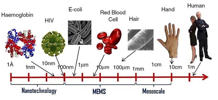
microelectromechanical systems (MEMS) are microscopic sensors, actuators and transducers with moving mechanical parts at the microscopic scale.
What is MEMS?
MEMS stands for micro-electro-mechanical system. It is also known by other affiliated names such as microsystems technology (MST) or micromachines. MEMS is an umbrella term for a wide range of microfabrication designs, methods and mechanisms that involve realising moving mechanical parts at the microscopic scale.
What are the uses of MEMS?
Microelectromechanical systems (MEMS) are used in various sensors, actuators, generators, energy sources, biochemical and biomedical systems and oscillators. Some examples of MEMS applications in engineering product design include:
- Sensors such as MEMS accelerometers, MEMS Microphones, MEMS gyroscopes, MEMS pressure sensors, MEMS tilt sensors and other types of MEMS resonant sensors
- Actuators such as MEMS switches, micro-pumps, micro-levers and micro-grippers
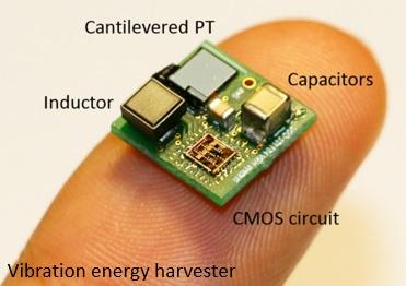
- Generators and energy sources such as MEMS vibration energy harvesters, MEMS fuel cells and MEMS radioisotope power generators
- Biochemical and biomedical systems such as MEMS biosensors, lab-on-chips, and MEMS air microfluidic and particulate sensors
- MEMS oscillators for accurate timekeeping and frequency control applications
The fabrication technology morphs into a nanoelectromechanical system (NEMS) at an even smaller nanometre scale. Furthermore, where MEMS is integrated with other technologies, various combinatory embodiments can take form, such as bioMEMS, where biochemical and biomedical systems are realised on microfabricated devices, micro-opto-electro-mechanical system (MOEMS) or OptoMEMS, where optical systems such as micro-mirrors are integrated to manipulate or sense light at the microscopic scale, radio frequency microelectromechanical system (RF MEMS) typically involves close integration with semiconductor microelectronics to provide RF transduction and switching capabilities.
Technological advancement of MEMS
The first laboratory demonstration of MEMS devices came about in the 1960s as a MEMS pressure sensor. Academic research gained momentum in the 1980s, while commercial development and manufacturing took off in the 1990s. Today, everyone carries MEMS devices on themselves in the form of smartphones, smartwatches and fitness trackers. In the past, an aeronautic gyroscopic system used to determine roll, pitch and yaw in the cockpit of aircraft weighed several kilograms and measured several inches in length, whereas nowadays, MEMS gyroscopes in our smartphones weigh less than a milligram and are equivalent in size to a grain of sand. With miniaturisation in size also comes a significant reduction in manufacturing cost and improved scales of economy. This is like the continued miniaturisation and reduction in cost seen in the semiconductor industry.
Advantages and disadvantages of MEMS
Advantages of MEMS
- Highly scalable in manufacturing, resulting in very low unit costs when mass-produced
- MEMS sensors possess extremely high sensitivity
- MEMS switches and actuators can attain very high frequencies
- MEMS devices require very low power consumption
- MEMS can be readily integrated with microelectronics to achieve embedded mechatronic systems – For example Microphones
- Scaling effects at microscopic levels can be leveraged to achieve designs and dynamic mechanisms otherwise not possible at macro-scales.
Disadvantages of MEMS
- Very expensive during the research and development stage for any new MEMS design or devices
- Very expensive upfront setup cost for fabrication cleanrooms and foundry facilities
- Fabrication and assembly unit costs can be very high for low quantities. Therefore, MEMS are not suitable for niche applications unless cost is not an issue.
- Testing equipment to characterise the quality and performance can also be expensive.
How are MEMS made?
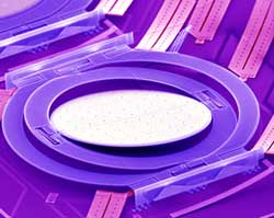
MEMS are classically micromachined from silicon. Various types of silicon wafers exist, and silicon can be doped to varying conductivity levels. Additional functional materials can be added to provide various capabilities, such as electrode layers or piezoelectric layers. MEMS design and fabrication involves a series of steps and cycles, which can be summarised into:
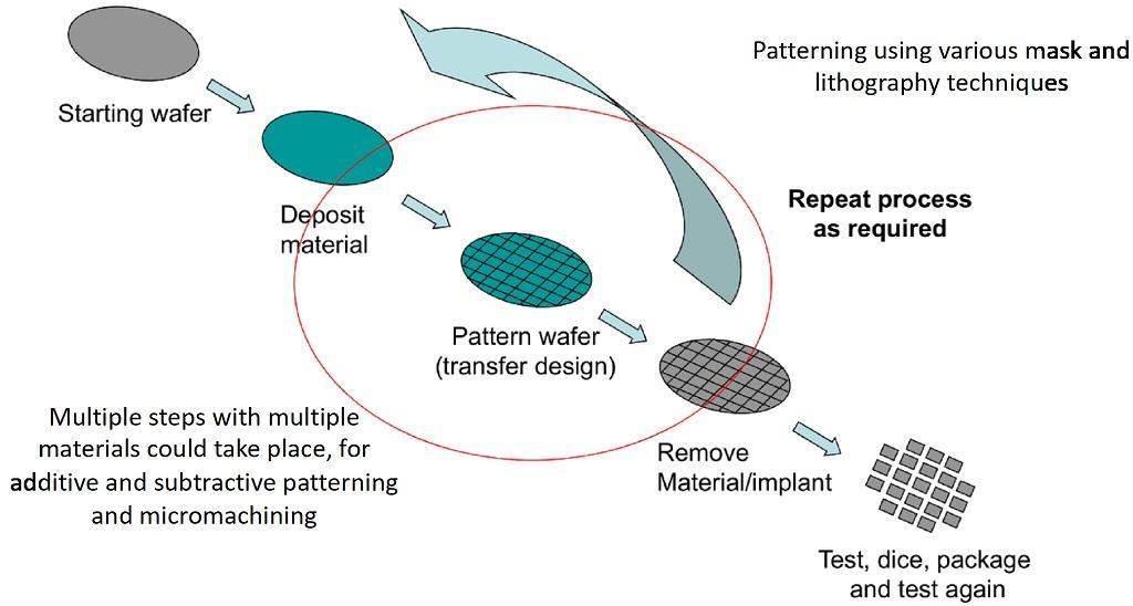
- Design, modelling and simulation (using analytical, numerical, CAD and FEA methods)
- Layout and wafer tape-out (using Layout Editor)
- Starting wafer substrate (such as silicon, glass, quartz, stainless steel, or plastics)
- Microfabrication process (cycling through the following steps until desired design is achieved)
- Additive (material deposition: chemical vapour, sputtering, evaporation, oxidisation)
- Pattern (masks, photolithography, contact lithography, projection lithography)
- Subtractive (material etching: wet chemical, dry ion or plasma, DRIE)
- Die dicing (laser, diamond saw, plasma etch)
- Wire bonding (to connect to interface circuitry)
- Packaging and encapsulation (hermetic seal, plastic/ceramic/metal seal, wafer-level packaging)
Types of MEMS transducers
To interact with the world, MEMS devices can employ various transduction mechanisms. Usually, these are mechanical-to-electrical transducers and vice versa so we can control the MEMS devices and their interactions with the mechanical world through interface circuits. Several other types of transducers can also be used to interact with chemical, light, magnetic, RF (Radio Frequency) and other domains.
Conventionally, electrostatic is the most popular transducer in silicon MEMS. This is because no additional specialist material is required, and micromachined silicon can be doped to provide conductivity. An electrostatic force can be sustained by establishing an electric field across a pair of capacitive parallel plates. When mechanical motion changes the distance between the parallel plates, an electrical signal can be measured across the parallel plates. Alternatively, the parallel plate can be actuated by applying a dynamic electrical signal. Comb finger designs are very popular amongst MEMS electrostatic transducers to maximise the capacitive surface area of the transducer.
In the past decade, piezoelectric transducers are also becoming more popular in MEMS design as fabrication technology for micromachining piezoelectric materials has improved. Typically, MEMS-compatible piezoelectric materials include aluminium nitride (AlN), zinc oxide (ZnO), sol-gel lead zirconate titanate (PZT), thinned bulk PZT, and various combinations of niobates. As the fabrication technology further matures, more functional materials can potentially be integrated with silicon micromachining processes.
Some of the main transducers used in MEMS include:
| Capacitive | Magnetostriction & Magnetic |
| Electrostatic | Radio-frequency (RF) |
| Piezoelectric | Thermal (temperature gradient or temperature fluctuation) |
| Ferroelectric | Optic (light energy or light signals) |
| Electromagnetic | Chemical (micro-fluidics) |
| Triboelectric | Biological and biomedical |
References and recommended reading
- Stephen D. Senturia, Microsystem Design, Springer US, 2001
- Mohamed Gad-el-Hak, The MEMS Handbook, CRC Press, 2002
- Nadim Maluf and Kirt Williams, Introduction to Microelectromechanical Systems Engineering, Artech House, 2004
- Mohamed Gad-el-Hak, MEMS: Applications, CRC Press, 2005
- James J. Allen, Micro Electro Mechanical System Design, CRC Press, 2005
- M. Edward Motamedi, MOEMS: Micro-Opto-electro-mechanical Systems, SPIE Press, 2005
- Wanjun Wang and Steven A. Soper, Bio-MEMS: Technologies and Applications, CRC Press, 2006